The Importance of SPI in Electronics Manufacturing
Introduction
Solder paste inspection (SPI) is a critical step in the production of printed circuit boards (PCBs), serving as a cornerstone for achieving high-quality and reliable electronic assemblies. As component densities increase and tolerances become tighter, the accuracy of solder paste application significantly impacts the success of downstream processes. Without effective SPI, defects introduced during paste deposition can result in costly rework, production delays, and reduced product reliability.
Why Solder Paste Inspection Matters
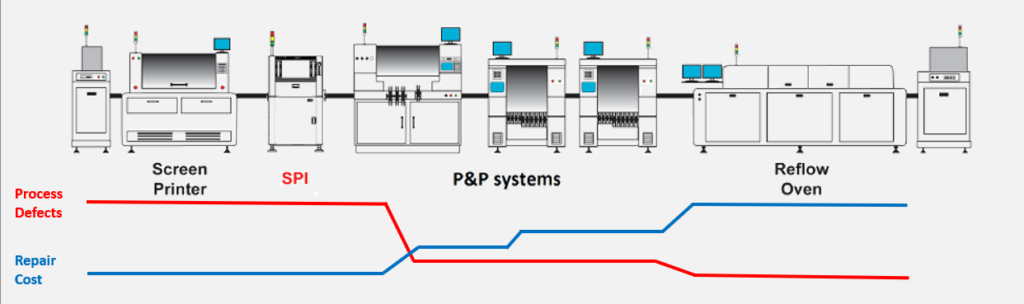
The solder paste printing process is one of the most delicate and error-prone stages in PCB assembly. SPI systems are designed to evaluate the volume, height, and alignment of solder paste deposits on PCB pads. These measurements ensure proper adhesion and electrical connections during component placement and reflow soldering.
Common defects such as insufficient solder paste, excessive paste, or misaligned deposits can lead to solder joint failures, bridging, or open circuits. Furthermore, some PCBs, especially those with high component density or critical functionality, are nearly impossible to repair after the reflow process. This makes early detection of defects through SPI not just beneficial, but absolutely essential for preventing irreparable damage and ensuring production success.
Benefits of SPI
- Improved Product Reliability:
SPI ensures precise solder paste application, reducing the risk of solder joint defects and enhancing product durability. - Cost Efficiency:
Early defect detection minimizes scrap and rework costs, saving significant resources.
- Optimized Process Control:
Advanced SPI systems provide real-time feedback, enabling manufacturers to adjust printing parameters and maintain consistent paste application. - Higher Yields:
Consistent and accurate solder paste deposition leads to fewer defects and improved manufacturing efficiency, especially in high-volume production environments.
Advanced SPI Technologies
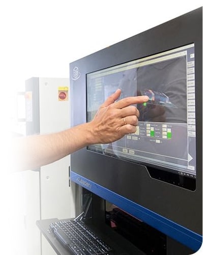
Modern SPI systems utilize cutting-edge technologies, including 3D imaging, to analyze solder paste deposits with unparalleled accuracy. Unlike traditional 2D inspection, 3D SPI systems measure paste volume, height, and shape, offering a more comprehensive analysis.
Companies like ALeader have pioneered advanced SPI solutions, incorporating proprietary algorithms and high-speed imaging to deliver precise and reliable results. These systems are designed to handle a wide variety of PCBs, from simple designs to high-density layouts, ensuring exceptional quality across different production requirements.
Conclusion
Solder paste inspection is an indispensable tool in modern electronics manufacturing, ensuring quality, efficiency, and reliability. By detecting defects early in the process and providing actionable insights, SPI systems contribute to cost savings, improved yields, and higher product reliability. As electronic assemblies become increasingly complex, adopting advanced SPI solutions like those offered by ALeader ensures manufacturers stay ahead in a competitive industry.